Project Idea: Low power Eink display

I’ve had this idea in mind for a while, an E-paper display that is connected to the internet.

In this blog post, I want to freeze the high-level idea and the project execution plan. Hacker/maker Extraordinaire Sprite_TM has done something before on similar lines. I’m planning to build my own version from scratch while adding some new features

I use a combination of physical sticky notes, along with the reminders and notes app on my Apple devices for improving my productivity at work and at home. I feel that it would be a great idea if could somehow combine these three tools into one device, and this is the first step towards it. Here’s a block diagram of my Idea.Capture

Here are the major components of the project

  1. the cloud app running on Digital Ocean VPS
  2. the Wifi to low power 2.4ghz radio bridge (Something like the Canny)
  3. The Epaper module(Hardware+Firmware)

The cloud app should be able to authenticate me and be able to get data securely via the API, I’m thinking of starting with OneNote web API as it seems to be easier to get started with. The output of this app would be a text file with some additional info (like date and some unique id for the target E-Paper display)

The bridge should be able to query the server and be able to translate the query from the display to a cURL call or something.

The Epaper module should have some intelligence and have the ability to query the bridge and display the text (or images). Also, I would like this module to have like a Name tag mode, would make for a cool conversation starter at Events/Meetups.

I’ll post detailed blog posts on each of the components as I finish them. This project has lots of components and involves putting together a lot of components. Also, secure communication between the three components would be an important part of the design.

The ‘Magic’ behind Fast Charging

The Idea for this post struck me on a hot summer day here in California, it was a 100F outside and my phone mounted on the car dashboard wouldn’t charge as fast(like 1% in like 30 minutes) although the phone indicated that it was in fast charge mode and I could not see any other issues with the charger or the charging cable, maybe the heat was affecting the charge rate?, I had to find out for myself.

There are two broad Fast charging technologies out there, Qualcomm’s QuickCharge and Oppo’s VOOC charging. Most mainstream smartphone brands use Quickcharge, while smartphone brands like Oppo and One plus use VOOC based charging technology. Both technologies are really interesting and solve the same problem using different approaches. This post is primarily about  Qualcomm’s quick charge 2.0, which was implemented in the Galaxy Note 4(circa 2014) that I had on hand. Newer phones use QC 3.0 or more recently QC 4.0.

Instrumentation: 

I came across this really neat little LTC2943 chip from Linear Tech (now part of Analog Devices). I think the target application for this chip is laptop Lithium Ion battery charge monitoring, but it should work well for this application.

The schematic is as shown below, basically, the Rsense is hooked in between the Charger Side Vbus and the Phone side Vbus

FastChargeMonitoringSchematic

I then needed a device that could talk to the LTC2943 and log the data to my computer over USB. Some Arduino code running on the Atmel Atmega328p Xplained Mini did the trick. The Xplained board also has debugging capabilities which made prototyping easier. the debugger onboard can also act as a USB to serial bridge so all I needed to do was ensure the output in proper format and I could copy the data from the serial terminal to a CSV for easier processing.

qc2.0_setup

The actual breadboard setup(this is a quick and dirty setup that I came up with, worked well for this test)

Once the instrumentation was in place I basically ran the test twice once with quick charge enabled and once without.

Analysis:

I wrote some quick python code to analyze the data from the two test runs. Check the screen capture below for the results

A few quick observations from the data (tl;dr):

  1. Quick charge seems to violate the USB Vbus voltage spec
  2. Quick charge uses the D+ and D- for voltage negotiation, hence you wouldn’t risk damaging a non-QC device by plugging into a QC compatible charger
    1. qc2.0LUT
  3. Quick charge algorithm seems to back’s off on the current under the following conditions
    1. When the phone is being used or if the battery is being loaded above a certain threshold
    2. when the temperature crosses a certain threshold, this is to prevent battery over heating
  4. Quick charge is less efficient than regular USB charging, this is evident from the higher amount of heat being dissipated by the end device

Additional references

  1. Interesting TI app note on implementing QC 2.0
  2. Github link to the firmware/software/hardware used for this experiment: https://github.com/hmms/fast-charge-analysis 

Fun with capacitive touch and low power circuit design

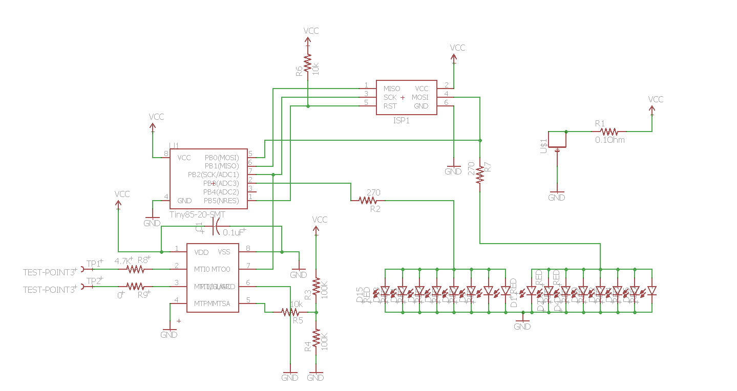
Recently, I built a touch activated LED toy based on the Attiny85V from Microchip (née Atmel). The schematic is shown below

Capture2

I got the PCBs made from every hobbyist’s favorite PCB manufacturer OSHpark. On the surface, the project seemed pretty simple. It gave me an opportunity to work on touch sensors and learn their functioning and implementation. I decided to go with an external touch sense solution(MTCH102 from Microchip as well), as I had plenty of board space to spare and, the it wouldn’t add much cost to the BOM. Also it would save me a lot of development time as implementing a robust power efficient capacitive touch library could be an interesting project in itself!

when starting with the project I set the following constraints:

  1. Cost < $12 (for qty < 10)
  2. Power (powered from a CR2032, the battery should last at least a month)

The cost target was an easy one, the most expensive component was the Attiny itself at around $2.25, other components were virtually “free” .

Meeting the power target though was a bit challenging. This post is mostly about how I was able to reduce the power consumption, mostly through firmware modifications.

  1. Utilizing the sleep mode was an obvious choice since that could improve the standby time of the device literally by orders of magnitude. I used the following setup to measure sleep current. Vd was the vdrop across the rather large shunt. This rather large shunt worked for me since I was only concerned about the sleep/standby current and the voltage drop across the shunt would be pretty minuscule across the resistor at such low currents (<1 mA).I used a Vichy VC99 DMM and my Rigol Ds1054z (this scope is amazing value for the money!, mine doesn’t play well with USB thumb drives though 😦 ) to measure and analyse the current draw.

14672717_10209036021752004_1999944468_o

2. on initial measurement through the DMM the current draw seemed be varying quite a bit, this took me down another rabbit hole of how the touch sensor actually functioned. the MTCH102 has a pretty interesting power down mode, and the datasheet doesn’t do it enough justice. I was using the aptly named Low-power mode in my implementation. which basically involved tying down the MTPM, low-power mode selection pin to ground

Capture

3. down the rabbit hole we go! It seems that the chip implements a pretty intersting psuedo-random algorithm to scan during the burst mode. the datasheet just calls it the burst scan. The chip sends out random length of pulses to the sense pad. The pulses are always in multiples of 16. And always between one and 10 sets of these 16 pulses are sent out.

14632733_10209036757250391_435003763_o

one set of pulses

14614398_10209036757450396_946820214_o

4. This reflected on the current draw was  as well, when the chip would be in burst scan mode the power consumption was up to 1.2mA. the scope capture below shows the Vd (across the 100Ohm shunt) when two sets of pulses were sent out through the sense pin.

14625802_10209036040992485_2080256186_o-1024x576

5. the only work around for this was to use the smart scheduling mode. This way I could control when the burst scan occurred, instead of every 256 ms i could set it occur say every second or so. I could go this route cut down the power consumption significantly! but then I would have to respin the board 😦

Capture1

6. but wait… the base line power consumption when the MTCH102 in sleep was still kinda high. about 300uA.  a google search later, is stumbled upon this app note about reducing power consumption on the AVR. one of the first things that they had mentioned was to enable the internal pull ups  on un used GPIOs to prevent power drain due to floating gates.  I had three unused GPIOs that were essentially floating, made changes to the code and viola! I was able to shave off ~100uA

Capture3

7. with sleep mode and implementing the internal  pull ups and disabling the  unused modules I was able to get the average current consumption to under 200uA. a typical CR2032 cell is rated for 240mAh. this would give me an estimated standby time of about 1200 hours (or 50 days). Also the internal resistance of the cell increases as its charge depletes. Also considering the device consumes ~20mA when awake for about two seconds. Assuming the device wakes up once a day, we should theoretically still have enough charge for a run time of over 30 days(240mAh – 0.03mAh- 144mAh = 95.97mAh leftover).

To conclude I think this project was an overall success and met its primary goals. There is some room for optimization and I think the power consumption can still be reduced further, but for now I think I should move on to the next project!

Hiking: Visit to Alamere Falls

Yesterday I visited Alamere Falls, near Bolinas,CA.

We started at the Palomarin Trailhead (there’s plenty of parking there, it being peak season though we had a hard time finding parking)

It’s a rather long hike (8 mi+)but large sections of trail have good tree cover and it was very foggy when we visited. do remember to pack as much water as you can and some energy bars.Note that there’s no clear sign or marking indicating the trail that leads to the waterfall. I suspect that this might be due to the fact that trail is quite dangerous and steep, and the authorities don’t want people to go there. I used the offline maps feature in here maps to find my way.

The way to get there from the trail head is as follows, Follow along the signs for coast trail, then take the Alamere falls trail, the trail length is around ~4.4mi from the trail head to the waterfall.

There are a few lakes on the trail as well, so pack some gear along if you plan on taking a dip.

Location on google maps for Alamere Falls.

Also if you’re driving from the south (through Stinson Beach)there a few scenic spots along the Bolinas lagoon waterfront.

Here are a few pictures from the trip.

Coast trail

Pelican Lake

Coast Trail

Alamere Falls

Bolinas lagoon waterfront.

Pasta sauce hack: How to make creamy tomato pasta the easy way.

It was a lazy Sunday afternoon, and I was craving something that’s tasty, but not too difficult to make and pasta sounded like a good idea. I really love creamy Alfredo sauce, but i had no parmesan cheese on hand. I also like tomato pasta sauce, but when made fresh. I really hate the taste of store bought pasta sauces, they are way too sour and leave a weird aftertaste. But these sauces are super convenient, so I always have them in stock.

So, the only stuff I had on hand was tomato (with garlic and basil) pasta sauce, heavy whipping cream and penne pasta. I cooked the pasta as per the instructions on the box, then drained the pasta. Heated some butter in the pan, added the tomato pasta sauce and while it was about to heat up added some of the heavy cream, garlic powder, dried basil leaves, and Voila!. the result was this awesome creamy, rich bright reddish orange pasta sauce, that was easy to make and tasted awesome(and looked beautiful too). I added some finely chopped cilantro to the sauce too, since I really love the taste of fresh cilantro.

20160724_153732

Working on a “secret” project, and fighting feature creep!

I started work on a new design, I have long had a desire to create a “product” from scratch using minimal off-the-shelf stuff. This design should help me achieve that goal, and help me learn project management(albeit on a micro scale! :P). Last year I spent some time on an esp8266 based design, new ideas got added to the design midway and a couple iterations later, i have OSHpark purple “art”. FEATURE CREEP,  as it’s called, its very hard to fight off.

This time i decided to start simple. The design has tight constraints (ultra low power consumption, dimesions) but fewer variables that might get affected by feature creep. I feel, I have mostly been successful to fight it off this time. I wouldn’t tell what the project is just yet, and i haven’t committed it to a public git repo yet(of course, it’ll be OSH). I shall make it public soon 🙂 . I think it’ll be fun, and hopefully I teach myself a few lessons in project management, and how to be persistent and finish my hobby projects!

In the mean time here’s a sneak peek of the schematic! 😀

Capture-2

Electronics Inside a Philips Sonicare Electric toothbrush

Today a coworker of mine gave me his old Philips Sonicare toothbrush. He said it had stopped charging and would no longer work. That was a good opportunity for a tear down 😉

Lets see what makes this baby chooch….(As the great man himself said https://www.youtube.com/watch?v=lA0kiYqyBmo)

12562858_10206868876974739_1096742337_o1

There’s very little to this device. it seems like there’s just a micro controller running the show, like every other product. (there’s more horsepower in a toothbrush these days than an a 50 year old Supercomputer!) it probably does the following tasks( my guesstimate)

  1. Running the motors
  2. Reading user input via the two push buttons (I accidentally De-soldered one Push button, while trying to De-solder the battery)
  3. Battery charging and discharging
  4. LEDs and Blinkenlights (Coz humans love ’em )

12544927_10206868900655331_127689890_o

Quick hardware analysis

A quick analysis of the PCB shows a micro controller(PIC16F726 to be precise) . Q1 seems to be a dual P channel MOSFET ( marked as ISC 6981D ). Q2 is marked AO8808A a dual N Channel MOSFET. The MOSFETs formed an H bridge which drives the “Ultrasonic motor” which I plan to get to run soon. then there’s a few sundry(read boring/uninteresting) components which probably are there for over voltage protection, an LDO, Li-Ion battery charger Etc. (High Res Image of the PCB ).

Then there seems to be 6 test Points which are conveniently labelled for easy debugging( or hacking I guess!) I’ll probe those and see what they do probably try out a few common baud rates and see what the Micro spits out. There are plenty of test points on the PCB that should include the programming pins for the micro as well.

That’s pretty much it for the electronics side of things.

Then there are other things like the Motor, A AA size Li-Ion battery, a charging coil. The coil probably forms an air core transformer with the charging dock, but I;m still not clear on how it is rectified back in to DC for charging the battery, with so few components and no bulky capacitors on the PCB.

I’ll probably power up the micro controller and see whats being sent out over the UART. Next on my To-do list would be to get the motor running and after that i would like to check out how the charging subsystem works with the weird air core coil arrangement. The weekend is fast approaching, so this guy should keep me busy for a good part of the weekend.

Special Thanks to Alex for donation 🙂

Murli’s blog has a new home

Last weekend over thanksgiving, I finally found some time to move over my blog to a custom hosted solution over from the old one. I now have a custom WordPress install(this might change soon, as I’m looking at other options, which are more efficient like jekyll ).  The blog should now be snappier, also i’m planning to add a few bells and whistles on the backend (git server, host some files etc). On the hardware front, I am currently working on the ESP8266 on adding an Epaper display and a few custom sensors. I’m using a rather interesting and firmware framework called SMING, which is an interesting hybrid between the Arduino framework and native GCC. Sming I feel is still rather nascent, but the developers are working hard on refining it. I plan to finish the e paper display interface this week, and then I can go ahead with finishing the project, something that looks more like a product than a quick hack. I’ve had a few stumbling blocks along the way, which i have put them aside for now.

Its been a long time dream of mine to build some thing that look more like a store-bought product than something hacked together. This is proving to be a much tougher and more resource intensive than I expected, but I’m being persistent and have been working on and off on it for a while now. Hopefully I will have something cool to show off soon, and will be richer with interesting experiences on developing a product from scratch. 

Also my Rpi Zero came in this weekend. I played around with it a bit, I’m waiting on some cables to come so I can have a stable setup, the cables from my previous Rpi hack are kinda dodgy and dont seem to work very well, I will post a detailed review on the Zero soon.

Raspberry Pi laptop

Recently, I got a used Atrix 4g lapdock for 30 bucks off of craigslist. It was a really good deal for a device that packs a USB hub, a 10+ inch LCD a keyboard, a trackpad and also a 10000mAh battery. Supply it with a processor and it can be a full fledged laptop computer. My atrix 2 worked fine with the lapdock. I used it a lot for watching youtube videos and for PDFs.

The good thing about the lapdock is that it has everything that is needed to setup a raspberry pi. I had one of the earliest revisions of the raspberry pi which up until now I used as my media file server. And the only was i would interact with it was over SSH since i really hated the mess of wires that would come with setting up the monitor and keyboard for the Pi. The lapdock was a very elegant solution to this problem. it was just a matter of splicing some wires together and some soldering before i would get my very own Rpi Laptop. Here’s the finished product.

1015455_10202044834936703_1783134473_o

If you are looking to make one below are some resources.

Here’s the instructional video from Adafruit that i referred to make this project. do check it out.

Here’s another blogpost which i think managed to do away with the soldering altogether but you might end up spending some extra money. but is more rugged and sturdy than the home-made cable solution. http://rpidock.blogspot.com/2012/05/raspberry-pi-and-motorola-lapdock.html

Here are the cables and stuff that you will need for this project.

1.      Micro USB B Male Female M/F Extension Charging Cable

2.     HDMI 1.4 D type Micro HDMI Male to Micro HDMI Female M/F

3.     HDMI Male to Micro HDMI Female Adapter/Converter

4.     Micro USB cable

You will also need Soldering iron and some heat shrink tubing for the project. So keep that handy.

Do let me know how it goes.

Questions?? Fell free to post them in the comments below!


Teardown of a 13 year old canon digital camera.

IMG_0685IMG_0684IMG_0686IMG_0687IMG_0688IMG_0689
IMG_0690IMG_0691IMG_0692IMG_0693IMG_0694IMG_0695
IMG_0696IMG_0697IMG_0698IMG_0699IMG_0700IMG_0701
IMG_0702IMG_0703IMG_0704IMG_0705IMG_0706IMG_0707

canon camera teardown, a set on Flickr.

A couple weeks ago, at work I found a digital camera that was thrown away in the recycle bin, it had a broken LCD and everything else seems to be in good shape. It was a 2.1 Megapixel Shooter so i figured it must really old. On googling I found that it was launched in 2001 and one of the smallest digital cameras of its time. and cost like $600 US! these days you can get a decent DSLR for that price. Check out the review of this device here!

Enough chit-chat, lets get to the real deal. I wanted to take the sucker apart and see the innards and understand its working. The camera is enclosed in a metal enclosure and could easily take a drop or two without taking much damage. Dissaembly was easy as the entire case was held together by philips head screws. The canon engineers were able to cram in a lot of stuff into a relatively tiny case,about the size of a pack of cards. It even had its own Li-Ion battery with a seperate external charger.

I have posted the photos of the teardown on my Flickr account. The pictures have elaborate descriptions feel free to browse through them. Feel free to ask any questions in the comments below! Enjoy!