I have a Dual Boot boot system Running Ubuntu 12.04(LTS) and Windows & Home Premium(x64).
The other day i was booted into ubuntu and had to use gparted to partition and format a flash drive to use with my Pogoplug-B01. And i by-mistake formatted the windows boot partition . Oops. I restarted my system and could not boot into windows! For me Windows is like a necessary Evil . Its where all my games reside! All for the other programming related stuff i use ubuntu. So i needed to get the windows partition up and running.
Also before you go ahead i would recommend you take a backup just in case anything goes wrong by booting into the system by a ubuntu live CD.
This can only be used to repair a system where the boot partition is either formatted or is corrupted. This would not work if the main system partition containing the OS itself is damaged.
Starting Windows Vista Microsoft made the boot partition a separate partition (generally 100MB)from the partition containing the actual OS files.
Step 1 Get the appropriate WIN 7 recovery Image from here.
Step 2 Create the CD/DVD or the USB stick(Skip to Method 2 in this Link )
Step 3 Without the boot sector When you turn on your computer u will get a ‘no Operating system Found’ error . So you will need to set your boot drive to the DVD or the USB drive Depending upon whta media you are using.
Step 4 Once you Boot into the Repair Disk Hit Startup Repair. If that fixes the issue. you are all set! But for me that was not so Easy. I Selected the Command Prompt Option the type in the following commands and hit enter after each command
diskpart
list disk
select disk (followed by the number of the OS disk; most likely 0)
list partition
select partition (followed by the number of the Boot partition; most likely the 100-200Mb partition)
active
exit
Step 5 Now again type
diskpart
list disk
select disk(followed by the number of the OS disk; most likely 0)
list partition
make Sure there’s a star(*) against the selected boot partition
then type format and hit enter. This will format the boot partition to NTFS.
Step 6 Now to repair the boot partition make the boot partition active by repeating the STEP 4
next enter following commands and hit enter after each command.
bootrec /fixmbr
bootrec /fixboot
bootrec /rebuildbcd
Step 7 Now restart the computer with the recovery media plugged in.
now in the recovery options select the ‘Startup Repair’ option. It should b able to fix any other issue with the boot sector and restore it to the optimal state.
Now Restart the computer and this time remember to unplug the media when the system shuts down.
I just started playing around with the TI Stellaris Launchpad a couple of days ago.
The Launchpad is a pretty powerful little dev board. It has ARM Cortex-M4F core at it heart. The really awesome thing is that there’s a Full fledged debugger built-in which makes it a really good board to start with ARM micros.
I was fiddling with the UART trying to setup two way communication with the micro. so i started out with the uart_echo project included in the Stellarisware bundle.
The uart_echo code works with the UART0 of the micro and i wanted to get it running on the UART1, Sound simple right? But for a Newbie to this micro-controller it might be a bit difficult. That was what happened it took some amount of digging around the internets and the documentation to get the code to do what i wanted but finally it started working
Here’s what i ended up doing. First i reconfigured all the I/Os the UART1 Pins can be used either on PB0,1 or on PC4.5. I used the PB0 and PB1 pins. changed the code in all the other relevant places in the main code, tried running the code . I got the “Enter Text” messgae on the terminal. It means the Tx was working fine. but i could get a echo back from the micro. The uart_echo uses the uart receive interrupt which was not being triggered. So i needed to get the interrupt triggered when the data comes in on the RX pin. by the way i did try the echo function running in the while loop and that confirmed that the physical connection was good and that the code was working.
I stumbled upon a forum post by another person facing similiar problems where he suggested that i make changes to the interrupt vector table in the startup_ccs.c file i simply replaced the IntDefaultHandler with the UART1IntHandler which is the interrupt handler for UART1 and like magic the code started working! Here’s the final Ti Code Composer studio v5.2 project. You can Import the code directly into CCS using the import option.
Planning to get the PWM working now…..will post on it soon…
Motorola launched the atrix 2 in india late last month. Almost six months after they launched it in the US.
It seemed like a good vfm phone given the market price of around 22,000 INR and the many positive reviews all around the internet made it seem like an awesome buy!!!
So i thought i should check it out.I ordered it,from probably india’s answer to amazon flipkart. it arrived 3 days post order. Packed snuggly in couple of layers of bubble wrap which i enjoyed popping! :P.
Lets open it up and check it out!
Overview
The atrix2 comes with pretty standard stuff inbox. A 2gig micro sd. A pair of earphones , that i will probably never use! A data cable. A charger with a USB socket. So that you can directly plug in your datacable into the charger and it becomes the charging cord! Most manufacturers now-a-days ship phones with a female usb so that people can just plug in the datacable itself and charge their phones!! I think its cool! The battery that comes with the phones a li-po battery with a capacity of around 1785mAh max(1735 mAh Typ.)! Thats awesome and reviews everywhere say that the large battery really helps a lot in keeping the phone alive and kicking for like more than a day, and with super heavy use! Infact the big battery and the dual core processor were the biggest factors that made me go for this phone!
Hardware
As i said the phone is powered by a dual core processor. Infact the phone is based on the TI OMAP4430 chipset with 2 arm-cortex A9 cores!! And the gpu is a powervr SGX540. The hardware was able ti handle 3d games pretty easily! I tested the 3D capabilities with the bundled EA games that came free with the phone. Dead space looked stunning and i was able to play the game without a single frame being dropped!
I also ran a few benchmarks with the Quadrant Standard Benchmark. And It scored a decent 1756. and Even bettered the galaxy nexus in the 3D scores.
The Sound quality was decent.The true Quality was not evident with the bundled Headset. But Sounded good on my Skullcandy Inkd Ear Buds.
The Display Is a qHD 960×540 TFT. The resolution and Pixel density is awesome .The colors appeared a bit yellow. Sunlight Visibility was okay. Overall the display is ok ,but a better quality display would have been much appreciated.
The Phone also Supports USB HOST.But i haven’t tried it out yet .Will be trying it out soon. And i will post about it soon,as soon as i’m done.There’s also a mini HDMI Jack for connecting to a monitor or a TV set. The cable is not bundled with the handset.
There are two camera one on the front for video chat and another on the back .The rear Camera has a 8Mp Sensor and has a single LED flash.Low Light performance is ok. Better than Most cameras. The images can be shot in various modes and at various resolutions. I liked the widescreen Image option Where the image is shot at a widescreen aspect ratio. and the resolution is around 6Mp.Full HD Videos can be Shot With the camera.Here’s a Sample of a Video that i took with the camera. (Thats Hemanshu Playing the bass Cover for Billy jean in the video).Videos Came Out Pretty good at 1080p and even at lower resolutions.Even at night the videos Came out pretty decent.Infact I think the videos came out better than the Images shot in low light!
Software
The Phone Comes with android gingerbread 2.3.6 out of the box. And a ICS update for the Asia pacific model (the models available in india) is expected in 3q 2012. That’s actually pretty late considering that most devices will be getting their ICS updates in 2q and there are already devices running Android 4.0 in the market!
Moto phones are bundled with their Custom version of the Android UI called MOTOBLUR,which i really like ,Much better than Samsungs Touchwiz UI which Is more like a clone of Apple’s UI. and even HTC SENSE which i don’t like at all.
The default Music Player App is Actually great in some aspects. It fetches the lyrics asn album art for you as the song is being played. It does not save the lyrics though hence to enjoy the lyrics you will need internet connectivity when the song is being played.It uses Tunewiki for fetching the song info.
There also this thing called the Universal inbox.Its basically a Place where all your unread Fb messages and texts are displayed in a single widget.Kinda Cool but haven’t used it much yet.
The Phone has on-board storage of like 8Gb. But it cant be used to store data files. Only application data Can be stored.Rooting can probably Solve this ‘issue’ and allow the on-board storage to be used more efficiently.
The Lock Screen interface is nice and i really like it.
There is Also the motorola phone portal that allows to sync your phone with your PC not only over USB but alos using wifi!! That’s actually Neat! You can manage all your data ,contacts and message .Using a simple Browser Interface. Internet explorer is the only browser supported to allow data Management though! :(.Other things such as Contacts and Messages can be managed with virtually any browser.
The Dialer interface and contacts app Kinda Sucks and takes time getting used to. And Unlike in HTC devices the Contacts from different sources such as facebook,twitter and your phone book are not merged but appear as separate contacts! WTF??. The Contacts App implementation of HTC was way better in this aspect!.It used to give me contact match suggestion and it even merged contacts from various sources automatically. So that if a person in on FB,twitter and Also is in my phone book.It appears as a single Contact. Instead of Multiple contacts!!!
You get 5 Customizable home screens.The Other UI elements are pretty much standard Android nothing much to add in this department!
Design
The Size of the Phone is perfect and Fits snuggly into your palms. The back of the phone is Rubberized and has a fabric like texture to enhance the grip.
4 standard Android Keys are present at the bottom of the LCD.
The Key placement should is a bit too close to the edges and would have been better if it was placed a bit higher. The Keys get accidentally activated when typing with both hands. And can interfere and reduce the typing speed drastically!. I strongly recommend some sort of body cover for this phone.The Phone Seems Slippery,Especially when using it single-handed.I used a silicon jelly case from amzer. It improved the usability drastically!.And Also got a more comfortable grip on the phone.
The Earphone jack is the Worst part of the design,i feel. I tends to scratch the surface of the earphone Plug . I tried it with a couple of earphones. And the Plugs of both the Earphones were scratched badly!.I really hate it very much!
The rocker keys for the volume and the camera key on the side of the device are wedge shaped and have a sharp edge.Its a bit difficult to press them due to the shape. But i guess one can live with that as its not that bad actually!
Bottom line: The Real Good stuff :battery life ,qHD display, awesome Hardware,Decent Camera. The Let Downs The Silly Earphone Socket,the Display Is a TFT-LCD(Blacks are usually just grays,If you own a phone with an AMOLED display You will Find the display weird because of the poor contrast ratio),The Phone’s Design really makes typing with both hands in landscape Mode difficult.The rocker keys at the side could have been better designed,the phone lacks grip and hence neccesitates a body cover fro the phone
This Video Review Helped me a lot in making my decision but i think they didn’t cover the downsides of the device well .
Disclaimer: All the views expressed are totally based on my personal experiences and i am not affiliated to nor was paid by any of the organisations/companies mentioned in the above post.
Here are few simple templates that you might use for documenting your source; easiest use is with e.g. Visual Assist X, or any other tool that allows you to add predefined templates to your source code. I use these template with VAX and shortcut set to “/*!”, with short descriptive names, thus I don’t need to remember many shortcuts and have all at reach of 3 key-clicks. 😀
And we finish off with a small list of simple tips.
RGB LED strips such as this are available for a low price.They are generally bundled with a IR controller and a power supply to power the LEDs and to change the color ,display various colour sequences etc.The IR Receiver is similiar to those used in TV and requires line-of-sight for reliable operation . I wanted the strip to be Controllable via a PC or a Mobile Phone.So I decided to make my own RGB LED strip Controller and to enable wireless control i used Bluetooth technology.The device can be controlled using a PC or a mobile phone with Bluetooth having a suitable graphical user interface.
The Hardware needed for this build is pretty simple and uses commonly found devices and may be salvaged from old electronics.
IRF640 N-Channel MOSFET(salvaged from an old Uninterrupted Power Supply-Thanks Kushal for that Dead UPS! )
Connecting wires ,Berg strips,etc.
12v 1A+Wall wart.
The Firmware for the ATmega8L micrcontroller was developed with Arduino 0023 and also with Arduino 1.0 (Can be downloaded for your OS of choice from HERE).The GUI for the Windows PC was Developed using the GTK+ toolkit using the python bindings available via pyGTK(Get it from here).The GUI was designed for running on nokia s60 devices using pyS60.
The arduino Firmware
The arduino is an awesome prototyping platform.Churning out prototypes from Ideas is very fast since all the hardware and other functions are pretty much abstracted out and only the Application Logic needs to be implemented.
The Firmware performs the following basic functions.Handle the communication routines,Control the LED brightness for each of the Colors RED,GREEN and BLUE and also be able to display the various sequences of colors of light.
I have a Arduino Duemilanove that came with an Atmega328P processor onboard.The Atmega 328P would have been an overkill for this project so i decided to replace it with an Atmega8L.The mega8 has only 3 v/s 6 PWM channels and 8K v/s 32K of flash program memory of the mega328.To verify the firmware I set up a simple testbench with three LEDs one each of RED GREEN and BLUE LEDs plugged into a breadboard connected to the Digital pins 9,10,11 of the arduino.These Correspond to the PWM Pins on the atmega8. The Communications with the controller was tested with the standard serial port given by the FTDI interface of the arduino.
Once The test bench was setup I could move on to Actually Writing the Firmware.The Setup section consists of all the PWM pins being set as Output and the Serial Port opened to Communicate at 9600 Baud.The Main while Loop has a Non-blocking delay section in which the Functions are updated at a User changeable delay.The more the delay the more slowly the color transition takes place and viz.This is necessary because if a delay is not present then the transitions would be so fast that it would appear as if the LEDs are blinking.I have NOT used the default delay function of the arduino library because of it blocking nature(Here’s a good article about Non-blocking code).The delay would block the processor by executing a number of instructions with a known execution time to get the specified time delay and only then execute the next instruction.This blocking delay would cause problems when data arrives at the serial port and the processor is busy executing the delay.Hence the data will be missed by the processor or will be processed only when the delay loop completes execution thus introducing lags between the user giving input and the suitable function being executed.Non-blocking Delay is hence used to prevent these problems and to provide reliable communication.And Precisely for this reason I have avoided Blocking codes in my Firmware.
The CellPhone GUI
The Cellphone GUI is a pyS60 script with five consecutive dialog boxes for mode selection,red value,green value,blue value and the update delay value respectively.The mode selection selects one of three modes.Mode 0 is the default mode will fire up if no bluetooth device is connected for control .In this mode the entire colour spectrum is traversed starting from red end of the spectrum.The transition goes on in a infinte loop.Mode 2 is a mode where each color namely Red,Green,Blue and White Respectively “breathe” i.e. the intensity of each color goes from zero to maximum and back to zero.Check out the Video to see it in action.The Mode three is the Color Chooser Mode. In this mode the User can choose the color.Set the value of the respective color from 0 for completely off to 255 for fully bright.
Also the Update delay can be set in milliseconds.This is used for setting the Delay Between Each color transition.the more the dealy the more slower will be the colour change. An update delay of around 5 to 20 milliseconds has a pleasing effect.
[Screenshot]The Pys60 Script Running on my S60 3rd Edition Nokia N78.
The PC GUI.
The PC gui was created Using PyGTK and UImanager Tools for GUI Creation. The PC GUI runs well on Windows (and probably also on Linux).I have tested it on my Windows Seven Home Premium 64-bit laptop .For Running the Application on Linux Small Amount of changes will have to be made ,Like changing the serial port label(on linux the PORT variable would be something like dev/ttyUSB0) etc. But other than that it would work fine on linux too.The GUI has three sliders for Color selection and a Bunch of radio Buttons for Mode selection.The Sliders are active only in the color selection mode.Check out the Source code included in the Zip file attached
[Screenshot]The Python Gui running on A win7 Home Premium x64 Machine
Hardware Design
the Hardware basically consists of a Atmega8L Microcontroller (with an Arduino Bootloader on-board which i have included in the sources.zip file) and three IRF640 N-channel MOSFETs ,One Each for Driving Each Color on the RGB LED strip .There’s also Lm1117 3.3V power regulator for powering up the Logic and a Berg connector for connecting the RX,TX,GND and VCC lines of the Bluetooth Module with the Atmega.I did Not make a schematic since i did not want to etch a PCB.Instead i just built the entire circuit on a perf-board and used flexible wire to build the circuit.The Entire Circuit is designed to be powered by an 12V DC Supply.I checked the Power Consumption of the entire circuit with a Multimeter and it was found to be around 1Amp.I used a 12v 2 Amp SMPS based supply.
I made My prototype on a perfboard here’s a Pic of the Top Side.
And the Bottom Side
Working on a PCB using toner tranfer technique to finalise the prototype. All the Python Source Codes and the Hardware schematics and the Layout Diagrams in Eagle Format are included in the attached Zip File .Feedback is appreciated!(Note:a ULN2803 and a 7805 are some extra components on the PCB shown above that i tried out during testing.But are not necessary in this circuit).
Here are some pics of the project in action.
Download all the required Source codes and the hardware design files from here.
Just a Simple code snippet that allows you to send a byte over a 8-bit wide parallel bus when using 32 bit devices such as those based on the ARM architecture.
While programming AVRs this usually would suffice to send a BYTE over a parallel 8-bit wide port.Here’s an avr-gcc example
PORTC = data;
But with the a 32-bit microcontroller For example the LPC1768 from NXP.
Each port is 32 bits wide and in order to send a byte over an 8-bit section of the 32 bit wide ports
a write to the PIN register of the respective port doesnt work.The Arm cortex-m3 has registers called SET,CLR,MASK and PIN for each of the ports.The purpose of the registers is pretty obvious and for more info refer to the datasheet of the LPC1768 .
now in order to send an 8 bit data over a section of the port beginning at byte number 19
sends the data over the 8 bit section of port 2 beginning from pin 19 to pin 26 of the LPC1768.
1.First the pins corresponding to all the ones present in the 8-bit data are set.
2.The data is exored with FF.This sets all the zeroes in the data to ones and all the ones to zeroes
3.Then the data containing the ones in place where the original data had zeroes is used to clear the port.Hence only those pins corresponding to the Zeroes in the data are cleared.
Recently the indian rupee joined the elite league of currencies that have their own unique symbol. The symbol is a combination of the devanagri ‘ra’ and also symbolises the roman letter R. the two stokes signifies the tricolour and the progress of the nation. here’s how u can use it in your emails and word documents.
Given below are the steps to use the new Indian Rupee Symbol as a Font in your word applications:
1. Download the attached font Rupee.ttf or Rupee_Foradian.ttf
2. Copy the font and paste it in “Fonts” folder in Control Panel.
3. Open any Microsoft Office application (For E.g., Microsoft Office Word). (See Figure 1.a)
4. Select the font type as Rupee or Rupee Foradian.
5. Click on ` (Grave accent) symbol. This key is just above “tab” button in your keyboard. (See figure 2)
6. You can see the new Rupee symbol in your office application.
Figure 1.a. Rupee Symbol in MS word
Figure 1.b. Rupee Symbol in Gmail application
Figure2. Grave Accent Symbol
Limitations:
The “Rupee.ttf” font is necessary to view the currency symbol. So as long as the new symbol is not encoded in to Unicode font by default,
we cant use the symbol universally.
Thanks to Foradian Technologies for giving these fonts as a free download to public
Last week i was alone at home since my parents had gone out to attend a marriage in mangalore.I was alone at home for about 10 days and had no college since there was our college ‘techfest’.i dont like attending ‘techfests’ on a shoestring budget,like the one in our college!!.there only a few things which fit into my definition of tech there!
So I was alone & bored and to get rid of my boredom and loneliness i wanted to do some fun project.i had a few hundred bucks with me,and i had an old luminaire (called jhoomer in hindi)-it had those bayonet mounted so called ‘zero watt’ incandescent bulbs. I consider incandescents a thing of the past as they are very inefficient and are energy guzzlers-they waste a lot of energy as heat.Infact they generate much more heat than they produce light!!!So i thought that replacing the incandescents with power LEDs which consume lower power and produce much more light.Also the light is much more soothing to the eye.
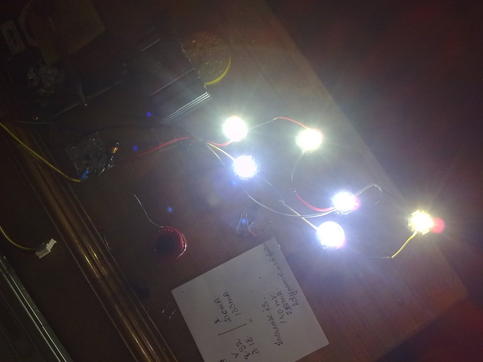
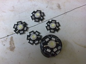
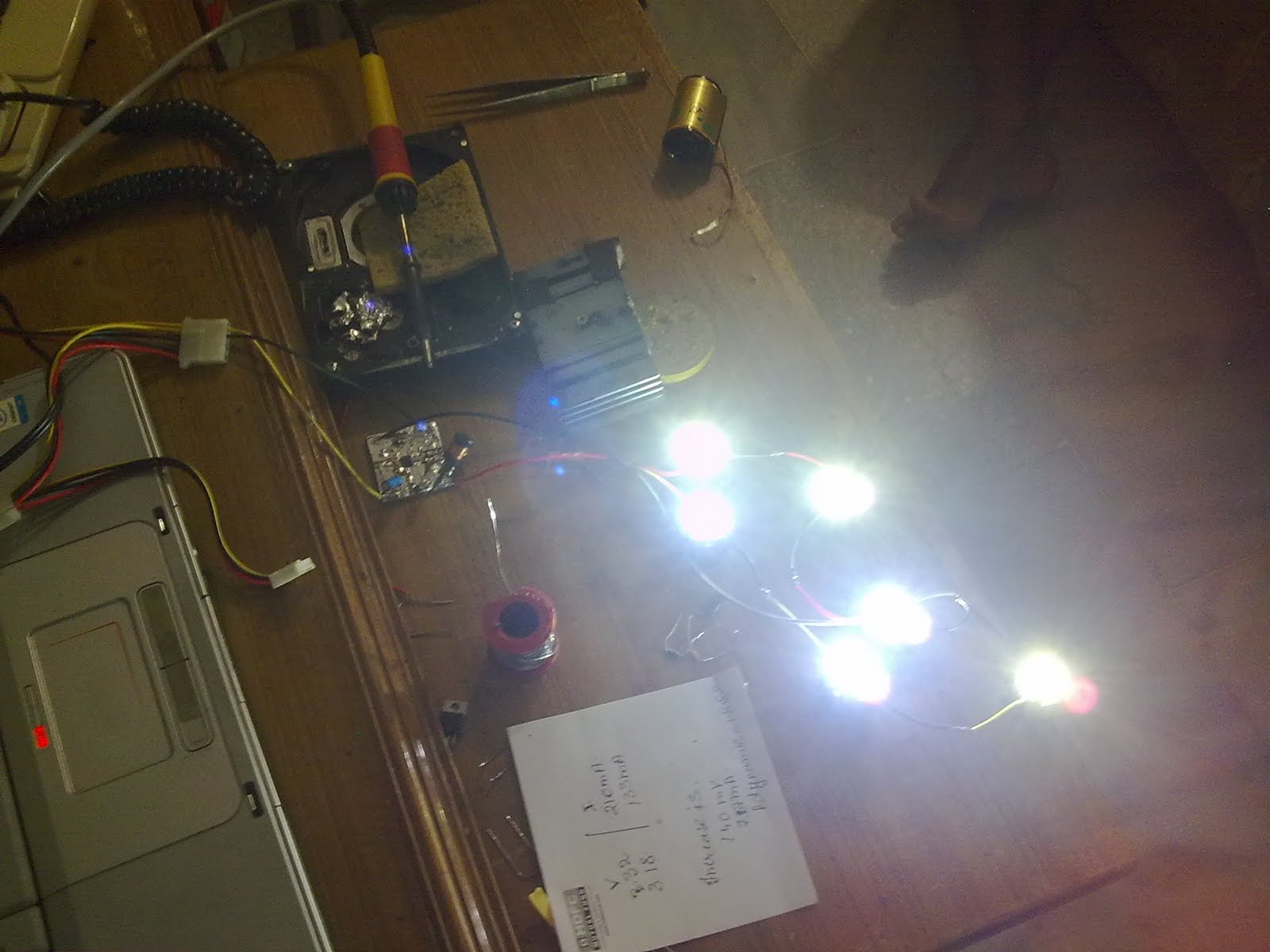
I went to the electronics heaven of mumbai-lamington road.with my friend Vijay to get some 1 watt LEDs.In my previous posts i have written about these LEDs and how to drive them.I got six 1 watt LEDs since my luminiare had six ‘arm’s.i could simply hook these leds to a wall wart of about 12 volts and a current rating of about 600 ma.hook it up in two parallel rows of three series LEDs .each LED requires a voltage drop of about 3.4v and a current of 300ma.that totals to about 10.2 volts and 600ma total power required. simple eh?? but that’s not the case these led are much more complicated devices as mentioned in the past posts.They require a constant regulated supply for stable and reliable operation. With the correct type of supply a long life can be expected of these LEDs.Usually these LEDs are rated for about 10,000 to 100,000 hours of operation.Thats miles ahead of the current fluorescent and incandescent technologies.
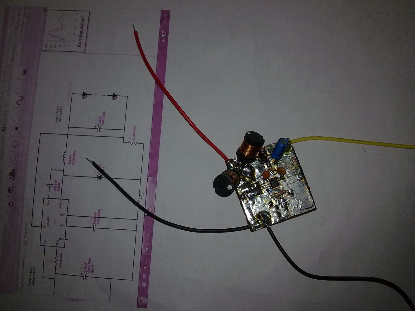
So i had to make the power supply for these LEDs so as to ensure reliable operation.I had a few LM3404 samples i had received from National semiconductor lying around.Its a buck converter based constant current source LED driver.It has an internal MOSFET capable to switch up an amp of current. requires very few external components for operation.Hence is ideal for my project.Also since it’s switching based device it has very high efficiency.So my objective of going green is fulfilled too.The rest of the components used have been salvaged from old electronics-old PC SMPS,old nokia charger,cordless phones,TV video games,FM radio,DVD writer etc.I firmly beleive in recycling!!.
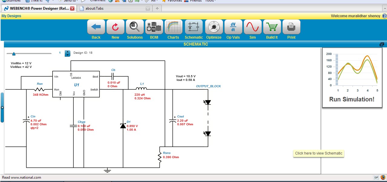
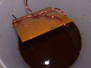
Now i checked out the datasheet of the LM3404,there were a lot of formulae and stuff on how to calculate the values of the various components used in the circuit.I found it difficult to get the accurate values of these components .I was also not too sure about the values being accurate. so i tried out the webench tools from National Semiconductor.These are great free tools from national which help in designing circuits based on their ICs.registration is required to use these tools which is also free. now on the webench designer page for LM3404 there were fields for the forward voltage of the LEDs,forward current,etc.I had no exact values for my LEDs since the guy whom i brought it from just referred to the as chinese made 1w led.So i assumed that it would be having a forward voltage of 3.4v and a current of 350ma.To confirm my assumption i had to check these specs with my multimeter.the volatge across the LED was 3.18v @133ma and 3.32v @210ma.I used a constant current supply mentioned in my provious post on power LEDs to check the voltage across the led.These values also help in determining the Rdyanmic-the dynamic resistance of the LED also known as ESR(equivalent series resistance).usually it is 1-2 ohms for power LEDs. In my case it was 1.81 ohms.The ESR can be calculated by measuring the increase in forward voltage drop dividedby the increase in current. For example, if the forward voltage drop increases by from 3.5V to 3.55V (a 50mV increase) when the forward current goes from 10mA to 20mA (a 10mA increase), the ESR will be 50 mV/10mA=5 ohms.I’ll be using a 12volt-1amp Wall wart from a deceased cordless phone as power souce for the LED driver cicuit.Take a printout of the circuit designed by the webench designer,as you’ll be needing it for further reference.here’s mine. there are 2 strings of three LEDs in parallel at the output block.
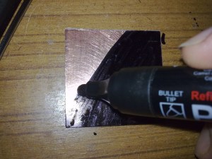
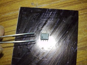
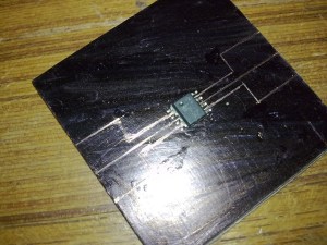
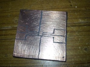
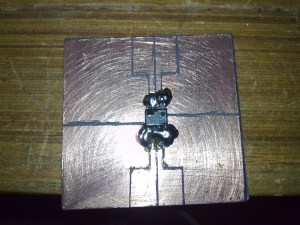
let’s start building the circuit now.The LM3404 chip was in a PSOP-8(power small outline package-8 pins)package.The SMD package is very tiny and i had to refer some sites to learn how to solder SMDs at home.The whole chip is just a couple of mm in width and in length!!I had to handle these using tweezers.First I placed the chip on a bare pcb coated with the ink from a permenent marker.
then i drew a few lines between the leads of the chip using the pointed end of one leg of the tweezer as shown.this exposes the copper of the pcb.Here the chip acts as the stencil.the chip can be held in place using an end of a toothpick.
extend the lines further and widen these lines if possible,to allow for use of thru hole components.now prepare the etching solution.I prefer ferric chloride. hold the pcb by means of a ‘holder’ i hav made one out of thick laminated copper wire.dip it into the etching soln.keep stirring continously.sometimes heating may also be required for speeding up the process.after the etching is done and all the bare copper is removed, remove the marker ink using acetone(sold as nail paint remover). your pcb is ready. check for any short circuits between the various parts of the pcb usin multimeter.i kept a small patch of copper shorted with the ground under the pcb to act as a heatsink since this chip has a powerpad at the bottom which is grounded.this power pad help dissipate heat as well as increase the sink/source capability of the chip.
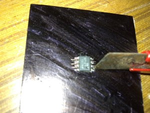
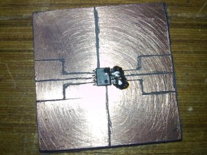
first of all hold the chip in place using a tootpick on the prepared PCB. solder just the pin no.1.this helps to keep the chip in place.now now solder the pin no.8. now the rest of the pin are soldered by placing a blob of solder on all the four pins on one side .then the blob maybe sucked out using desoldering braid which leaves only the required quantity of solder on the pad.the process is repeated on the other side as well. check for the continuity between the pads and the pins by a multimeter,once confirmed.proceed to soldering the other components.
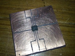
slightly bend the legs of the thru hole components then tin them.then solder these components over the
now try applying a thin layer of solder over the pcb.this helps in increasing the current carrying capacity of the pcb as well as to prevent oxidation of the copper.solder the components on the pcb as shown.a thin sticky layer of slag was formed on the pcb while soldering.this can be easily removed by rubbing a peice of cotton soaked in acetone.
i use this technique to ‘surface mount’ thru hole devices.this technique is great for prototyping.this method can also be used for ‘permanentizing’ the circuit. heres the completed circuit. before testing the circuit do remember to remove the slag as i can form a capacitor between the pins.this stray capacitance can damage the circuit and lead to malfunction and i learnt this the hard way.I had to sacrifice a IC to this stray capacitance :(.
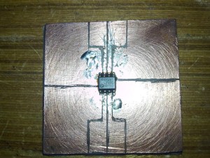
the led driver circuit is ready now.
Now these LEDs cary a huge amount of power for their size.They generate some heat so heat sinking is required to prevent any damage due to overheating.I got some small heatsinks that could fit in the bulbholders themselves so there’s no need to reengineer the LED mount.the LEDs were ‘stuck’ to the heatsinks by means of heats ink compound.a small container of this thermal compound would suffice and the cost just 10 bucks.i would suggest polishing the surface of the heatsink before applying the thermal paste.It is not necessary though.Just to be on the safer side i polished the surface of the heatsink with some sand paper.a very small amount of thermal paste is applied on the heatsink.so as to form a very thin layer. the LED is the placed on the heatsink and a small amount of force may be applied so as to place the LED firmly in place.this step is repated for all the leds.
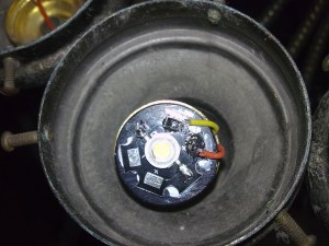
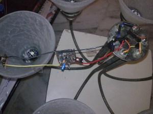
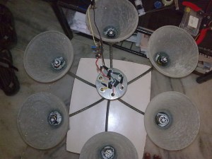
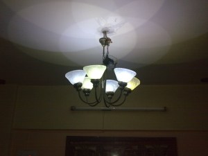
i managed to squeeze the LEDs fitted with the heatsink into the bayonet mountings of the incandescent bulb.this made my job of mounting the LEDs a bit easy.a lot of improvisation might be needed here.i also rewired the whole Luminaire. since the wire was old and was oxidised. i connected the each set of 3 LEDs in series. this gave me 2 strings of 3 series LEDs. i connected these two strings in parallel. i first tested the circuit with the 12v out from an computer SMPS.the yellow wire from the SMPS is the +12v while the black wire is the ground. the test was sucessfull so i proceeded to mounting the circuit.i attached a barrel plug connector to driver circuit so as to allow the connection of a standard wall wart supply. i used a 12v-1amp adapter that was used as a supply for a cordless phone. i mounted the circuit on the wallwart itself with some insulation tape.the supply for the adapter is given from the mains .after testing the circuit for another hour to check the stability i reassembled the luminaire and hung it back up on the ceiling.
Note:i was unable to upload the photos of soldering the through hole components on the SMD pcb due to some technical glitches.sorry for the incompleteness.will upload the pics as soon as possible.Also thanks to mandar for staying up late until the wee hours of morning and for that can of redbull which helped me stay up that late 😉


